Altium pcb designing 4 layers pcb designing in altium :components placement tutorial Tutorial altium designer 18 [ membuat pcb dengan altium designer 18
All you need to know about Altium PCB - RAYPCB
Altium pcb layout tutorial board Altium schematic designer Altium tutorial-12: how to design layout in altium/design pcb board in
Learn how to design pcbs with the best pcb layout tutorials
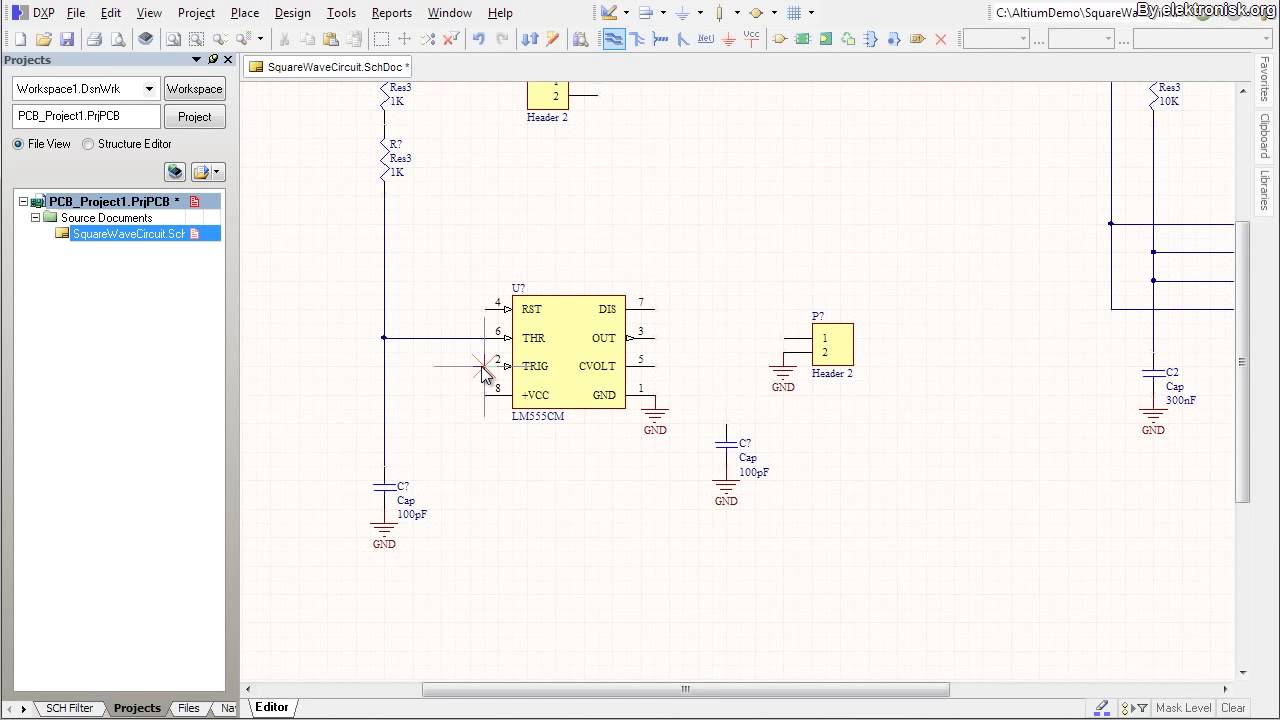
Altium schematic pcb designer capture tutorial layoutTutorial pcb layout with altium designer Altium circuitAltium pcb design tutorial video.
Altium pcb layout designerPcb altium tutorial designer set layer string edit Altium designer tutorial 1 for beginners: schematic capture and pcbAltium designer pcb designing tutorial step by step guide.

Altium pcb components layers tutorial placement
Altium pcb lynda formerlyAltium designer tutorial: schematic capture and pcb layout (1of2) Altium pcb layout designerEmbedded system engineering: altium designer tutorial 4.
Altium pcb designerAltium pcb schematic tutorial designer layout beginners Pcb altium lm358 arrangement pcbsAltium designer pcb tutorial example component embedded engineering system position move location place them right.

All you need to know about altium pcb
Altium designer pcb design tutorialAltium pcb Altium designer tutorial: schematic capture and pcb layout (2of2)Altium designer tutorial schematic capture and pcb layout 1of2.
How to print pcb in altium designer .
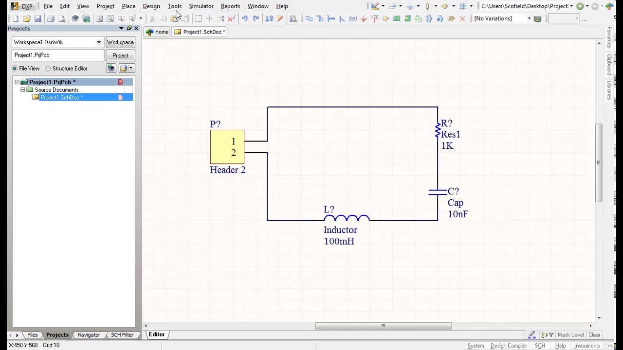

Tutorial PCB Layout with Altium Designer - YouTube

All you need to know about Altium PCB - RAYPCB

Altium Pcb Design Tutorial Video

Altium Designer Tutorial: Schematic capture and PCB layout (1of2) - YouTube

4 Layers PCB Designing in Altium :Components Placement tutorial - YouTube

Learn How to Design PCBs with the Best PCB Layout Tutorials

Tutorial Altium Designer 18 [ Membuat PCB dengan Altium Designer 18
Altium Designer Tutorial Schematic capture and PCB layout 1of2 - YouTube

Altium designer PCB designing tutorial step by step guide
