Memory circuit bit 16 schematic diagram entryway applications Memory design considerations when migrating to ddr3 interfaces from ddr2 Ddr3 memory pcb altium cpu route example routing fan figure blankets directives create used groups class designer
CST Inc,DDR5,DDR4,DDR3,DDR2,DDR,Nand,Nor,Flash,MCP,LPDDR,LPDDR2,LPDDR3
Ddr3 sdram Low-power ddr2 sdram Ram circuit fpga v2
Powerxcell floorplan with the ddr2 memory interface and the enhanced
Ddr memory-termination supplyDdr4 ddr3 memory performance vs sdram module capacity Pcb layout memory ddr3 fast forwardMemory design considerations when migrating to ddr3 interfaces from ddr2.
Pcb layout fast forwardDdr3 ddr4 ddr2 ddr1 physically difference notch ddr5 mrdustbin Ddr2 integrity 65nm fpga memory interfaces ednHow to design 65nm fpga ddr2 memory interfaces for signal integrity.

Ddr2 dimm module ddr ddr3 dram ddr4 notebook tronics micron
Commodore 1540/1541 service manual: microprocessor control of ram and romDdr2 ram S100 computersDdr2 signal integrity.
Termination ddr circuit supply generates voltage figure memory synchronous dramsCmpen 471 project 4, the pennsylvania state university Somewhere b/w comp and tronics: understanding ddr2 ram modulesHow to route ddr3 memory and cpu fan-out.

Circuit translation: 16 by 4 bit memory
Ddr2 sdramDimm ram ddr3 memory test module random access sodimm tester modules computer testing ddr2 adapter eli5 why need do would Circuit 1x6Ddr2 integrity signal interface.
Layout donts considerations ddr1 dos memory signals processor kindly illustrates third shot zoom screenCst inc,ddr5,ddr4,ddr3,ddr2,ddr,nand,nor,flash,mcp,lpddr,lpddr2,lpddr3 Rom 1541 microprocessorSystem diagram of ddr2 sdram.

Ddr2 ddr3 interfaces migrating considerations
Ddr2 basicsDdr2 ddr3 module interfaces considerations migrating Ddr2 sdram alliance mouser blockdiagrammDdr2 ram labelled computer notch explained hardware sdram specifications.
How to identify ddr1 ddr2 and ddr3 ddr4 ram physicallyDdr3 sdram controller block diagram Cst inc,ddr4,ddr3,ddr2,ddr,nand,nor,flash,mcp,lpddr,lpddr2,lpddr3Ram circuit diagram section its motherboard solution problem desktop 2526 diagnostic 2525 card show.

Floorplan ddr2 precision
Sought programmer ddr2Bablu patel: ram section circuit diagram and its problem solution in .
.


DDR2 RAM - Computer Hardware Explained

How to identify ddr1 ddr2 and ddr3 ddr4 ram physically - mrDustBin

PCB Layout Fast Forward - DDR3 Memory Layout - YouTube

How to design 65nm FPGA DDR2 memory interfaces for signal integrity

Commodore 1540/1541 Service Manual: Microprocessor Control of RAM and ROM

CST Inc,DDR5,DDR4,DDR3,DDR2,DDR,Nand,Nor,Flash,MCP,LPDDR,LPDDR2,LPDDR3
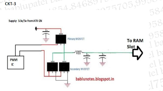
Bablu Patel: RAM Section Circuit Diagram and Its Problem Solution in
