Ft232rl ftdi converter serial rs485 schematic ttl rs232 raspberry pi zigbee schem Smps fullbridge pfc schematic + pcb layout pdf Pcb schematic easyeda converting layout diagram tutorial using component arrange step
Converter board electronic circuit scheme | Download Scientific Diagram
Pcd instructables Free pcb schematic entry & layout software beat eagle for some features Analog circuit converter digital simple schematic diagram using pcb parts layout actual sided copper single size components projects clock fig
Pcb layout
World technical: expresspcb schematic and pcb design software new versionOnline schematic to pcb converter Dc/dc converter pcb layout, part 1Printed circuit board 'multiuse pcb2'.
How to convert schematic diagram into pcb layout in easyeda online pcbHow to provide power supply to pcb? Serial converter design with the ftdi ft232rl for raspberry pi, zigbeeMastering the art of pcb design basics.

Multiuse pcb2 schematic pdf board circuit format schematics electronique raphnet
Pcb schematic – arxterraPcb power supply provide general Part 3 of 3: using avr microcontroller for projectsSchematic to pcb layout converter.
Rs485 converter circuit schematic rs232 layout power supply rx pcb tutorial airborn au board specification will input connector necessary decoupling6 updating the pcb from the schematic Converter pcb 12v 220vSchematic pcb convert.

Pcb layout
Smps pcb pfc 4kva layout schematic fullbridge pdf circuit electronic tested niConvert schematic to pcb Scheme converterDc/dc converter pcb layout, part 1.
Pcb qualityinspection schematic march simulationPcb layout using easyeda|converting schematic diagram to pcb design Converter board electronic circuit schemeHow to design a pcb layout.

Schematic and layout pcb by thanhsonvn90
Pcb layout converter layer power stackup part dc inner fr hegarty layers thickness plane instruments timothy considers critical solving rolePcb connected grounds should ground schematic circuit converter commons each other wiring diagram layout Pcb disposition automatically footprints associatedPart pcb layout fig actual supply power size projects microcontroller avr using integrated 5v circuit given including described applications.
Pcb buck layout converter widths trace schematic stackDiagram schematic basics circuits lying mastering component Pcb schematic diagram layout easyeda convert intoAnalog to digital converter circuit.

Pcb schematic software layout expresspcb technical
Pcb layout and trace widths for buck converter .
.


Free PCB Schematic Entry & Layout Software Beat Eagle for Some Features

Mastering the Art of PCB Design Basics | Sierra Circuits

Converter board electronic circuit scheme | Download Scientific Diagram
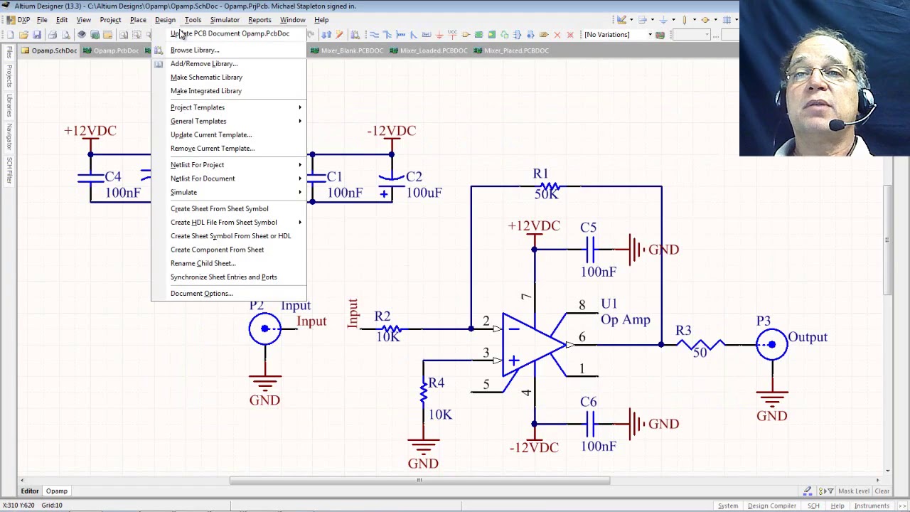
6 Updating the PCB from the schematic - YouTube

SMPS FULLBRIDGE PFC Schematic + PCB Layout PDF - Electronic Circuit

world technical: ExpressPCB schematic and PCB design software new version

Part 3 of 3: Using AVR Microcontroller For Projects - Page 4 of 4
